- 您现在的位置:买卖IC网 > Sheet目录342 > MB85R256FPFCN-G-BNDE1 (Fujitsu Semiconductor America Inc)IC FRAM 256KBIT 150NS 28TSOP
MB85R256F
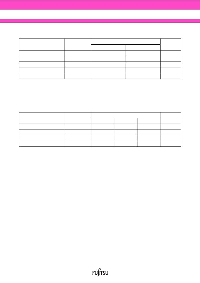
■ ABSOLUTE MAXIMUM RANGES
Parameter
Power supply voltage*
Input voltage*
Output voltage*
Operating temperature
Storage temperature
Symbol
V CC
V IN
V OUT
T A
Tstg
Min
? 0.5
? 0.5
? 0.5
? 40
? 40
Rating
Max
+ 4.0
V CC + 0.5
V CC + 0.5
+ 85
+ 125
Unit
V
V
V
° C
° C
* : These parameters are based on the condition that V SS is 0 V.
WARNING: Semiconductor devices can be permanently damaged by application of stress (voltage, current,
temperature, etc.) in excess of absolute maximum ratings. Do not exceed these ratings.
■ RECOMMENDED OPERATING CONDITIONS
Parameter
Power supply voltage*
High level input voltage*
Low level input voltage*
Operating temperature
Symbol
V CC
V IH
V IL
T A
Min
2.7
V CC × 0.8
? 0.5
? 40
Value
Typ
3.3
?
?
?
Max
3.6
V CC + 0.5
+ 0.6
+ 85
Unit
V
V
V
° C
* : These parameters are based on the condition that V SS is 0 V.
WARNING: The recommended operating conditions are required in order to ensure the normal operation of
the semiconductor device. All of the device's electrical characteristics are warranted when the
device is operated within these ranges.
Always use semiconductor devices within their recommended operating condition ranges.
Operation outside these ranges may adversely affect reliability and could result in device failure.
No warranty is made with respect to uses, operating conditions, or combinations not represented
on the data sheet. Users considering application outside the listed conditions are advised to contact
their representatives beforehand.
DS501-00011-1v0-E
5
发布紧急采购,3分钟左右您将得到回复。
相关PDF资料
MB85RC128PNF-G-JNE1
IC FRAM 128KBIT 400KHZ 8SOP
MB85RC16PNF-G-JNE1
IC FRAM 16KBIT 1MHZ 8SOP
MB85RC16VPNF-G-JNE1
IC FRAM 16KBIT 400KHZ 8SOP
MB85RC64PNF-G-JNE1
IC FRAM 64KBIT 400KHZ 8SOP
MB85RS128APNF-G-JNE1
IC FRAM 128KBIT 25MHZ 8SOP
MB85RS64PNF-G-JNE1
IC FRAM 64KBIT 20MHZ 8SOP
MC10SX1130DR2
IC LED DRIVER LINEAR 16-SOIC
MC33152DG
IC DRIVER MOSFET DUAL HS 8SOIC
相关代理商/技术参数
MB85R256FPF-G-BNDE1
功能描述:IC FRAM 256KBIT 150NS 28SOP RoHS:是 类别:集成电路 (IC) >> 存储器 系列:- 标准包装:1 系列:- 格式 - 存储器:闪存 存储器类型:闪存 - NAND 存储容量:4G(256M x 16) 速度:- 接口:并联 电源电压:2.7 V ~ 3.6 V 工作温度:0°C ~ 70°C 封装/外壳:48-TFSOP(0.724",18.40mm 宽) 供应商设备封装:48-TSOP I 包装:Digi-Reel® 其它名称:557-1461-6
MB85R256FPNF-G-JNE2
制造商:FUJITSU 功能描述:
MB85R256FPNF-G-JNERE2
制造商:FUJITSU 功能描述: 制造商:FUJITSU 功能描述:IC FRAM 256KBIT 150NS 28SOP
MB85R256G
制造商:FUJITSU 制造商全称:Fujitsu Component Limited. 功能描述:256K-bits FRAM LSI using the ferroelectric process and CMOS process technologies
MB85R256GPF-G-BNDE1
制造商:FUJITSU 功能描述:
MB85R256H
制造商:FUJITSU 制造商全称:Fujitsu Component Limited. 功能描述:Memory FRAM CMOS 256 K (32 K 】 8) Bit
MB85R256HPF
制造商:FUJITSU 制造商全称:Fujitsu Component Limited. 功能描述:Memory FRAM CMOS 256 K (32 K 】 8) Bit
MB85R256HPFCN
制造商:FUJITSU 制造商全称:Fujitsu Component Limited. 功能描述:Memory FRAM CMOS 256 K (32 K 】 8) Bit
